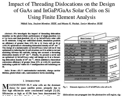
We have investigated the impact of TDD on the performance of 1J n+ p GaAs and 2J n+ p InGaP GaAs cells on Si at AM 1.5G spectrum. The analysis indicates that in a 1J GaAs cell on Si with a 2.5-μm-thick GaAs base. an efficiency of greater than 23% can be realized at a TDD of 106 cm−۲ . For both 1J and 2J cell configurations. the onset of degradation in Voc was found to occur at a lower TDD than in Jsc . indicating that Voc was more sensitive to TDD. The 2J InGaP GaAs cell at a TDD of 106 cm−۲ exhibited an efficiency of 26.22% with a 2.5- and 0.9-μm-thick GaAs and InGaP base. respectively.
The design of the 2J InGaP GaAs cell on Si was optimized at a TDD of 106 cm−۲ to achieve current matching between the two subcells. By thinning the top InGaP cell from 0.9 to 0.38 μm. the 2J cell efficiency increased to 29.62% from 26.22%. In addition. at the interfaces in the top InGaP subcell. the SRVs below 104 cm s had negligible impact on the 2J cell performance. Thus. even in a lattice-mismatched 2J InGaP GaAs cell on Si with TDD of 106 cm−۲ . a theoretical conversion efficiency of greater than 29% at AM1.5G is achievable by tailoring the device design. Once experimentally realized. the III–V cell technology on Si would offer a new paradigm for the advancement of low-cost III–V solar cells and foster innovative avenues for both space and terrestrial applications.
 Iran Energy News Oil, Gas, Petrochemical and Energy Field Specialized Channel


